Electronic design – PCB LAYOUT
Are you looking for a design house in electronic hardware and IoT ? We are acclaimed by many worldwide customers …
Anthemis Technologie‘s , we have chosen to be in efficiency and performance . Our team of engineers and passionate developers works conscientiously to achieve your electronic project.
Our company leader in the development market IoT offers you a high quality professional response for the success of your project.
Design of electronic boards and
development of embedded systems
development of embedded systems
We develop systems IoT and electronic boards ex-nihilo or starting from technological bricks.
According to the technical specifications that we draft with you, we select the best of the electronic components taking into account the requirements of the project.
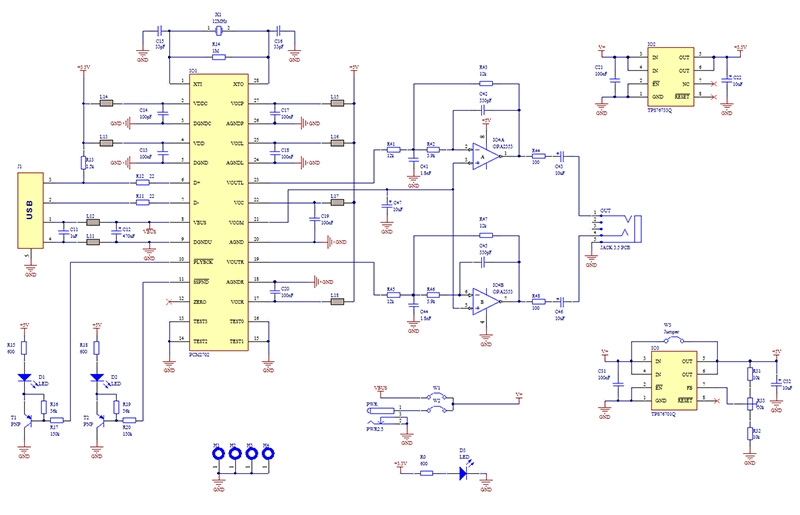
We calculate and establish the architectures and electronic diagrams that will make it possible to realize your IoT system.
Through our Software Engineering service, we drive electronics by designing the source code, firmwares and low level drivers required by Bones on board / RTOS .


Targets and technologies used:
- µC 8/16/32 bits ( STM32 , Atmel, Freescale, Texas, MicroChip…)
- ARM7, ARM9, ARM11, Cortex, SnapDragon
- Communicating objects: Bluetooth, Ble, SigFow, WiFi, Lora, Gsm, 4G
- Analog electronics (sensors, Sensors)
- Power electronics (Motors, Drivers, Chargers)
- Digital electronics (µC, CPU, FPGA and CPLD or SOC)
- Bus and networks (USB, CPL, CanOpen, Profinet, Ethernet IP)
- HMI and all ‘visual’ electronics (screen, panel, etc.)
- Energy management (NiMh battery, CdNi, LiPo …)
Need an electronic design?
PCB design – Printed circuit board layout
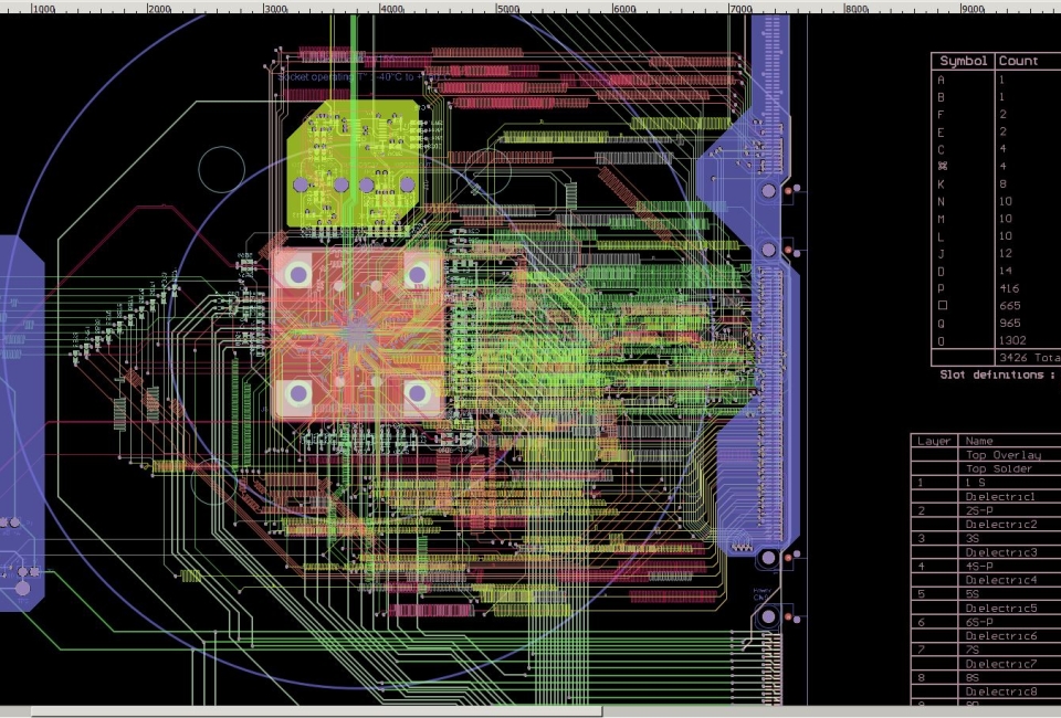
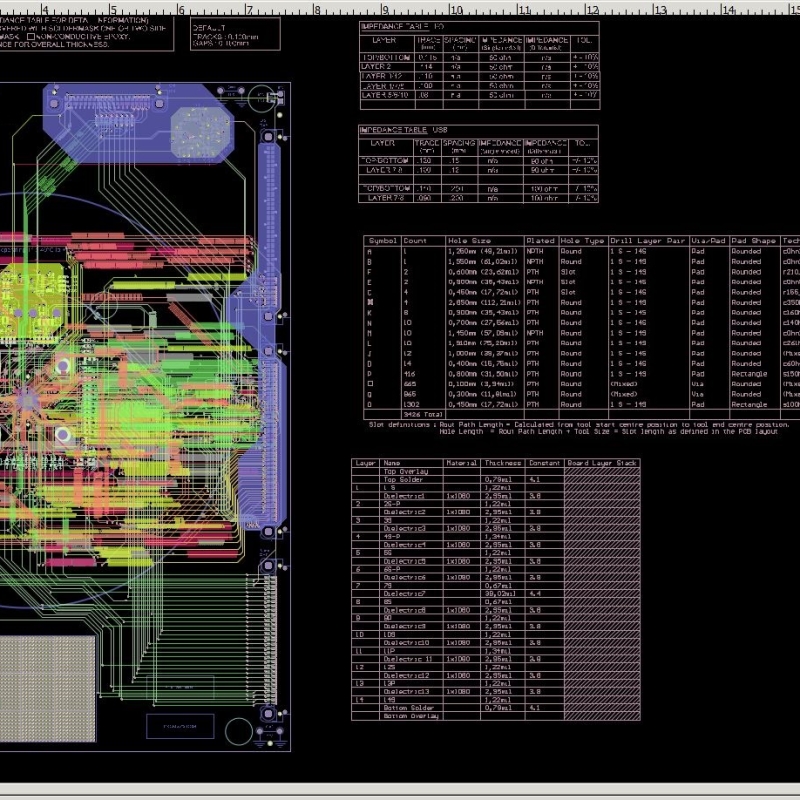
From the economical single-sided card to the complex multilayer printed circuit, Anthemis Technologies is at your service for the Routing / Layout of PCBs.
To succeed in this step, Anthemis Technologies has high-performance software resources (dedicated workstation) and a team of engineers and CAD designers High level PCB .
CAD constraints: HDI, adapted impedance, thermal and dimensional problems, industrialization requirements, EMC / LV and R & amp; TTE qualification , circuit testability,… are part of our skills.


Altium Designer and Protel – Zuken Cadstar and Visula or CR5000 – Pads Pcad – Proteus – Eagle – Orcad and Cadence
The electronic design CAD PCB integrates the entry of the electronic diagram , the placement and routing after a rigorous analysis of your specifications taking into consideration all the environmental parameters of the electronic board.
Each step of the CAD design ( diagram , floorplan, routing ) is subject to validation with the client.
At the end of the project a complete file is provided to you. This includes the technical file of wiring of the electronic board , the file of PCB manufacturing.


